Introduction
A few months ago, my embedded systems experience was limited to collecting temperature and accelerometer data on an ESP32-C3 dev board using Rust. Coming from a computer science background, I had written plenty of C++ code and JavaScript in my first jobs out of college, but aside from school studies I didn’t know much about the hardware side of things. I noticed the ESP32-C3-DevKit-RUST-1 dev board and decided try it out, but working with pre-built development boards only showed me half the picture.
I wanted to understand the why behind the hardware: Why does I²C require pull-up resistors? Why does my carefully written Rust code fail when the PCB layout is flawed? To answer these questions, I embarked on designing my own 2-layer STM32F103 breakout board in KiCAD 9 (on GNU/Linux, of course). The board includes pinouts for SWD, UART, I²C, and GPIO. This journey was a crash course in humility, teaching me that schematic optimism is no match for LCSC’s inventory constraints. Footprint reviews and BOM checks aren’t just best practices—they’re the difference between a functional PCB and hours of frustration with a soldering iron.
Design
Why STM32F103?
I chose the STM32F103 microcontroller for its affordability and versatility. It’s part of the ARM Cortex-M3 series, offering a solid balance of performance and peripherals. With its rich feature set, including SPI, I²C, UART, and GPIO it was perfect for my project.
Power Delivery
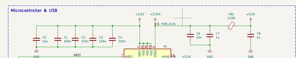
The first step in the design process was laying out the power delivery section of the schematic. Proper power delivery is critical for stable operation. I included 100nF and 10µF decoupling capacitors (C1–C8)—one pair for each VDD pin on the IC. These capacitors help filter noise and stabilize the power supply. Additionally, I added a 120Ω ferrite bead (FB1) to filter power on the analog side, ensuring clean power delivery to sensitive components.
Placement is key. In the PCB layout, these capacitors and the ferrite bead are positioned as close as possible to the microcontroller. This minimizes inductance and ensures reliable power delivery, allowing the microcontroller to boot up as expected.
Reset Circuit (NRST)
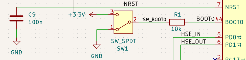
The NRST pin is connected to ground through a 100nF capacitor for electromagnetic shielding and to prevent parasitic reset issues. STM32 microcontrollers have an internal pull-up resistor on the NRST pin, so it can be left floating. For my use case, I’m relying on the SWD pinout for flashing and debugging, making the NRST pin less critical. However, I labeled the NRST net in the schematic for easy identification during PCB design.
Boot Mode Configuration (BOOT0)
The BOOT0 pin is connected to a 10kΩ series resistor and a single-pole double-throw (SPDT) switch. By default, the switch grounds BOOT0, allowing the microcontroller to boot from flash memory and execute its program. When the switch is toggled to 3.3V, BOOT0 is pulled high, enabling the bootloader for firmware flashing. This simple configuration ensures flexibility during development.
High-Speed External Clock (HSE)
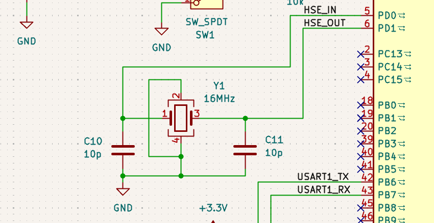
To improve timing accuracy, I opted for a 16MHz crystal oscillator as the HSE clock source. The oscillator is paired with two 10pF load capacitors to ground. Depending on your oscillator’s specifications, you could use capacitors in the 5pF–25pF range for your project. I calculated the load capacitance using the formula:
Here, accounts for stray capacitance, typically around 5pF. For optimal performance, the stm32f103c8 datasheet mentions that capacitors should be placed as close as possible to the crystal to minimize distortion. Later in the PCB layout images you’ll see what I mean by this. I labeled the oscillator nets as HSE_IN and HSE_OUT for easy identification during PCB layout.
Pinout Design
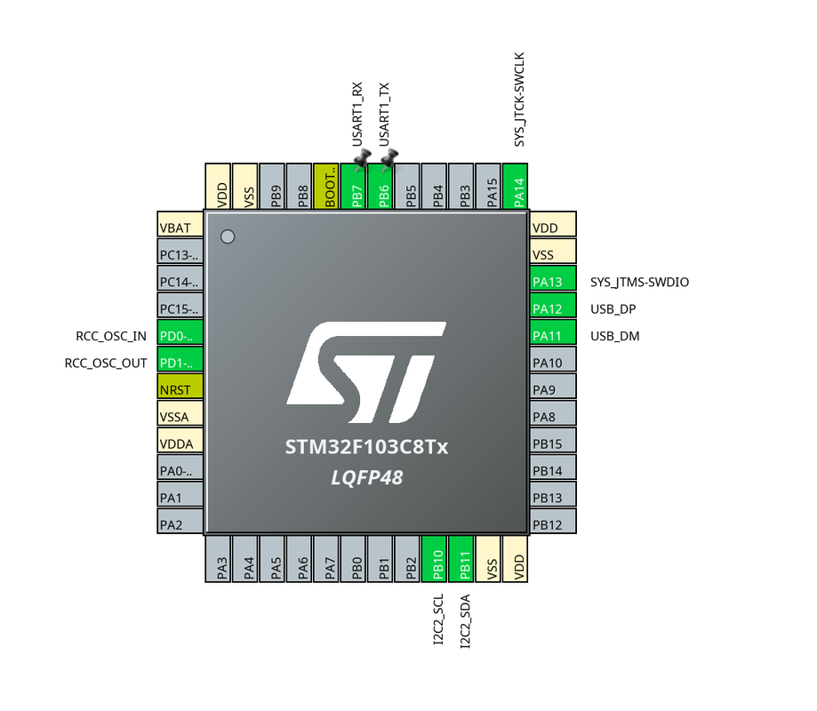
The pinout includes connections for SWD, UART, I²C, and GPIO. Each pin is labeled clearly in the schematic to simplify PCB layout and firmware development. I moved the USART pinouts from their original spot near the USB pin to where they are in the image near the BOOT0 pin. The two pins for the USB differential pair are pinned out to PA11 and PA13, with the SWD pins are at PA13 and PA14. Proper pinout design by using STM32CubeIDE ensures compatibility with debugging tools and external peripherals, not to mention an easier time with making the schematic with peripheral pin-outs in the first place.
PCB Layout
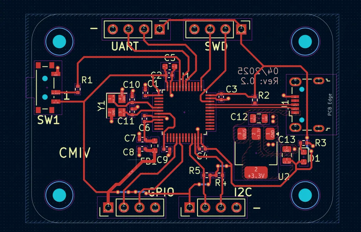
The schematic design so far has gotten us to this point, where we route the traces and place the components on the PCB itself. The power supply and step-down from 5V to 3V3 lives on the right side of the PCB with the necessary capacitors net labeled C12 and C13. The HSE labeled Y1 has its required capacitors in close proximity, those are labeled C10 and C11. The rest of the ceramic decoupling capacitors are very close to the IC power pins and allow the device to function as intended.
There are four male headers for the GPIO, SWD, I2C, and UART pins. I’ll be able to use jumper wires with a breadboard to do testing and debug the software. 3V3 power is routed to each of these headers with a corresponding ground pin. The I2C header in particular has 1k5 pull-up resistors so that the logic level is 3V3, it will be at that voltage when no data is being transferred. I’ll probably make a bi-directional level converter to use here later so that it can properly use a 5V powered device.
Assembly
Once the design was finalized, I exported the Gerber files from KiCAD and sent them to JLCPCB for manufacturing. JLCPCB offers affordable PCB fabrication and assembly services, making it an excellent choice for prototyping. However, I learned the hard way that even with professional assembly services, attention to detail during the design and BOM preparation stages is crucial to avoid headaches later.

Double-Checking the BOM and Parts
One of the most important lessons I learned during this process was the importance of thoroughly reviewing the Bill of Materials (BOM). While JLCPCB provides an extensive inventory of components, not every part in your schematic may be available. In my case, I overlooked the availability of the USB connector I had specified in the design. As a result, I chose to have JLCPCB assemble the boards without the USB component, leaving me to source and solder it manually on each PCB.
While this was an unexpected challenge, it turned out to be a fun and rewarding experience. Soldering the USB connectors myself gave me a deeper appreciation for the assembly process and the importance of component selection.
Tips for Avoiding BOM Issues:
- Check Inventory Early: Before finalizing your schematic, cross-reference your components with JLCPCB’s inventory. Their online tool allows you to search for parts and verify availability.
- Use Common Components: Whenever possible, choose widely available parts to reduce the risk of sourcing issues.
- Mark Critical Components: Highlight essential components in your BOM, such as connectors, voltage regulators, and crystals, to ensure they are prioritized during assembly. Use spreadsheets if needed and plan this out.
- Plan for Substitutions: If your preferred component is unavailable, identify suitable alternatives and update your schematic accordingly.
Preparing for Manual Soldering
If you find yourself in a situation where certain components need to be soldered manually, here’s what I did and the steps I took to make the process smoother:
- Source the Missing Components: I ordered the missing USB component from a reliable supplier, such as Digi-Key or Mouser in the United States. I made EXTRA SURE that the component now matched the footprint on the PCB.
- Gather Tools: I used a fine-tip 40W soldering iron, flux, tweezers, and solder wick for precision work. A magnifying glass also helped quite a bit here.
- Practice on a Spare PCB: If you’re new to soldering, practice on a spare PCB or prototyping board to build confidence.
- Follow a Workflow: Start by cleaning the pads with flux, positioning the component using tweezers, and soldering one pin to secure it. Then, solder the remaining pins, ensuring good contact and avoiding cold joints.
In my case, soldering the USB connectors manually was straightforward. The footprint was well-designed, with ample space around the pads for easy access. I found the process enjoyable, and it gave me a sense of accomplishment knowing I had contributed to the assembly process directly.
Final Assembly Checklist
Before sending your design to JLCPCB, use this checklist to ensure a smooth assembly process:
- Review the Schematic: Double-check all connections, especially power delivery and critical signal paths.
- Verify Footprints: Ensure all components have correct footprints and match the parts in your BOM.
- Inspect the PCB Layout: Check for issues like overlapping traces, misaligned solder masks, or insufficient clearance.
- Cross-Reference the BOM: Confirm that all components are available in JLCPCB’s inventory or plan for manual soldering.
- Generate Assembly Files: Export the pick-and-place file and assembly drawings to guide JLCPCB during the manufacturing process.
Lessons Learned
Designing a custom PCB is as much about planning as it is about execution. Here are some key takeaways:
- Inventory Constraints: Always check component availability before finalizing your schematic.
- Documentation Matters: Clear net labels and pinout diagrams save time during PCB design.
- Placement is Critical: Proper component placement minimizes noise and improves reliability.
Next Steps
With the basic STM32F103 breakout board complete, I plan to:
- Expand Functionality: Add features like SPI and CAN bus for more advanced projects in a later board revision.
- ESD Protection: Add and place correctly components that mitigate elecrostatic discharge.
- Develop Firmware: Write reusable libraries for peripherals in Rust.
Stay tuned for updates and the first Rust program that I flash to the device!